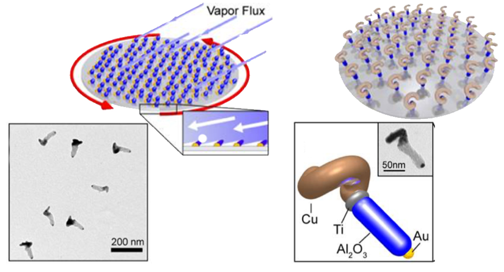
Schematic of vapor deposition under glancing angles onto b) a wafer to form complex 3D nanostructures, TEM images, and intended structure and actual nanostructure (inset).
3D Nanofabrication: nanoGLAD
Dhruv Singh, Melanie Adams, Johannes Sachs, Conny Miksch, Peer Fischer
Former members: Hyeon-Ho Jeong, Andrew Mark, John Gibbs, Tung-Chun Lee, Sahand Eslami, Debora Walker
We have advanced physical fabrication methods, such that they can be used for the rapid growth of hundreds of billions of nano-structures. Unlike any other growth method, it can combine multiple functional materials in one and the same complex 3D nanostructure.
No method has hitherto achieved truly complex solid 3D structures with full material flexibility at this scale. We use a known highly parallel and fast patterning method (Block Co-polymer Micellar Nanolithography) to deposit nanoparticles from solution at the wafer scale. These are then used as seed points for a physical vapor shadow (glancing angle) deposition. Under computer control and cooling the substrate can be manipulated, angled and rotated, such that discrete nano-structures grow in a highly parallel fashion on an entire wafer (see Figure). We can easily program shapes and the resultant structures are uniform. We use aour fabrication setups to grow designer nanostructures for a range of projects, e.g.:
- Nanopropellers
- Photonic nanoantennas
- Chiral plasmonics
- Protected nanocolloids
- Nanocolloids
- Chemically active nanomachines
- Magnetic nanostructures
- Thin films and coatings
“Hybrid nanocolloids with programmed 3D-shape and material composition”, A.G. Mark, J.G. Gibbs, T.-C. Lee, P.Fischer, Nature Materials 12, 802 (2013).
"Nanohelices by shadow growth", John Gibbs, Andrew G Mark, Tung-Chun Lee, Sahand Eslami, Debora Schamel and Peer Fischer, Nanoscale 6, 9457-9466, (2014).
“Dispersion and shape engineered plasmonic nanosensors”, H.-H. Jeong, A.G. Mark, M. Alarcon-Correa, I. Kim, P. Oswald, T.-C. Lee, P. Fischer, Nature Comm. 7, 11331, doi:10.1038/ncomms11331 (2016).
"Chiral nanomagnets", Sahand Eslami, John G Gibbs, Yvonne Rechkemmer, Joris van Slageren, Mariana Alarcón-Correa, Tung-Chun Lee, Andrew G Mark, Geert LJA Rikken, Peer Fischer, ACS Photonics, 1 (11), pp 1231–1236, (2014).
“Selectable nanopattern arrays for nanolithographic imprint and etch-mask applications”, Hyeon-Ho Jeong, Andrew G. Mark, Tung-Chun Lee, Kwanghyo Son, Wenwen Chen, Mariana Alarcón-Correa, Insook Kim, Gisela Schütz, and Peer Fischer, Adv. Sci., 2: 1500016. doi: 10.1002/advs.201500016 (2015).
